1. Overview
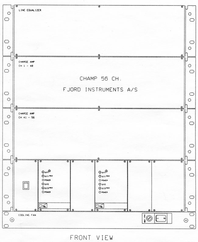
Fig. 1. Equalizer / Charge Amplifier front view The system comprises both equalizer and charge amplifier. 2. EqualizerIn an analogue streamer the sensor (hydrophone) signals are transmitted through twisted wire pairs to the instrumentation system. These wire pairs deteriorate the signal due to distributed capacitance and resistance along the way. The signals coming from the far end of the streamer will, of course, suffer most. The role of the equalizer is to make all streamer channels appear equally 'bad', seen from the head of the streamer. It does so by inserting a resistor-capacitor network into the signal path of every channel, simulating a certain length of a twisted wire. The nearest hydrophones will have the largest equalization. The resistor-capacitor values will then gradually decrease until there seems to be an equal distance of twisted pair wire between every hydrophone in the streamer and the next element in the signal processing chain (i.e. the charge amplifier).
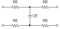
Values of RE and CE depend on the particular streamer in use. This survey uses Geco HSSG type active sections with these equalizer related parameters:
Each signal channel can have different component values. In practice, however, equalization is applied section wise - e.g. channel 1 to 8 will have identical RE/CE values, so will channel 9 to 16 etc. Equalizing one 100 m HSSG section using nearest component values yields RE = 10 ohm and CE = 6.8 nF.
|
|||||||||||||||||||||||||||||||||||||||||||||||||||||||||||||||||||||||||||||||||||||||||||||||||||

| Channel range | RE [ohm] | CE [nF] | Comments |
|---|---|---|---|
| 1 .. 8 | 20 | 15 | Mimics two HSSGs |
| 9 .. 16 | 10 | 6.8 | Mimics one HSSG |
| 17 .. 24 | 0 (strap) | 0 [remove] |
2.3: 25 m GL, 5 *
100 m active HSSG (20 channels)
The component values for this case is given below.
| Channel range | RE [ohm] | CE [nF] | Comments |
|---|---|---|---|
| 1 .. 4 | 40 | 15 || 15 = 30 | Mimics four HSSGs |
| 5 .. 8 | 30 | 15 || 6.8 = 21.8 | Mimics three HSSGs |
| 9 .. 12 | 20 | 15 | Mimics two HSSGs |
| 13 .. 16 | 10 | 6.8 | Mimics one HSSG |
| 17 .. 20 | 0 (strap) | 0 [remove] |
2.4. Equalizer PCB
There are 12 channels per board.
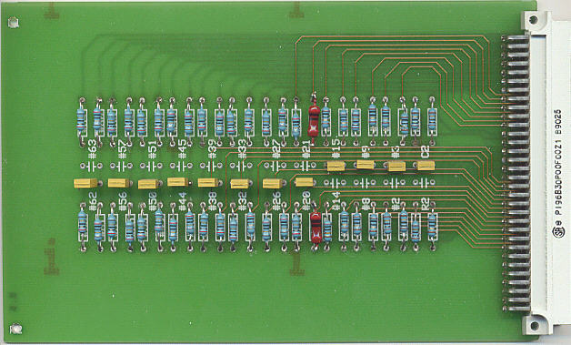
Fig. 3. Equalizer Printed Circuit Board (PCB)
|
3. Charge Amplifier
A charge amplifier is a current-to-voltage converter. It is needed because the hydrophone group has a very high output impedance - when it's circuit diagram using electric equivalents is drawn it is represented by a voltage source in series with a capacitor. An ideal charge amplifier has zero input impedance. This is a nice match for this type of signal source.
Each Charge Amplifier board is furnished with two differential charge amplifiers.
3.1 Circuit diagram
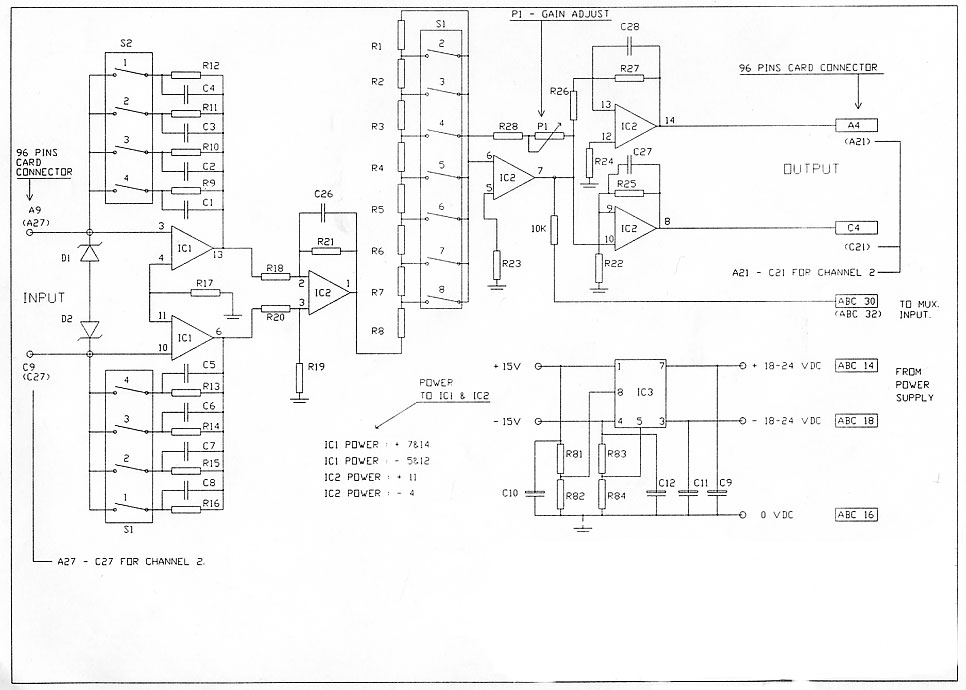
Fig. 4. Charge Amplifier circuit diagram. Two of these on each PCB. Click to enlarge.
Diagram is explained in the manual (can be downloaded, see below).
3.2 Gain equation
The gain equation for a differential charge amplifier is given by:
![]()
- Where
-
SO1 = Sensitivity [Volt/Bar] after charge amp, normally 100
V/Bar
CG = Group capacitance [nF]
CF = Differential charge amp. feedback capacitance values [nF]
SG = Group sensitivity [Volt/Bar]
The gain expression is used to calculate CF, see result in table below.
3.3 Low cut filter
The differential charge amplifier also includes a low cut filter by placing a resistor RF in parallell with CF (denoted R9 .. R16 in the circuit diagram). For a cut-off frequency fc = 3 Hz we can calculate RF by the expression:
RF = 1/(2¶*CF*fc)
The CF and RF values reflect the specific streamer and Group Length being used. For the GECO HSSG active streamer section the relevant parameters are given below, together with calculated values for CF and RF. SO1 = 100 V/Bar.
| HSSG parameters | Calculated values | |||
|---|---|---|---|---|
| Group Length | SG [Volt/Bar] | CG [nF] | CF [nF] | RF [kohm] |
| 12.5 m | 68 | 45 | 61.2 | 866.8 |
| 25 m | 68 | 90 | 122.4 | 433.4 |
3.4 Switches and layout
Switches for Group Length (GL) setting (unmodified cards, ref. section below):
- First channel: S1 and S2. Second channel: S5 and S6:
Position 1: 6.25 m GL
Position 2: 12.5 m GL
Position 3, 4: Not used.
Switches for gain setting (sensitivity):
- First channel: S3, Second channel: S4
Position 2 on: 10 V/Bar
Position 3 on: 15 V/Bar
Position 4 on: 20 V/Bar
Position 5 on: 25 V/Bar
Position 6 on: 50 V/Bar
Position 7 on: 75 V/Bar
Position 8 on: 100 V/Bar
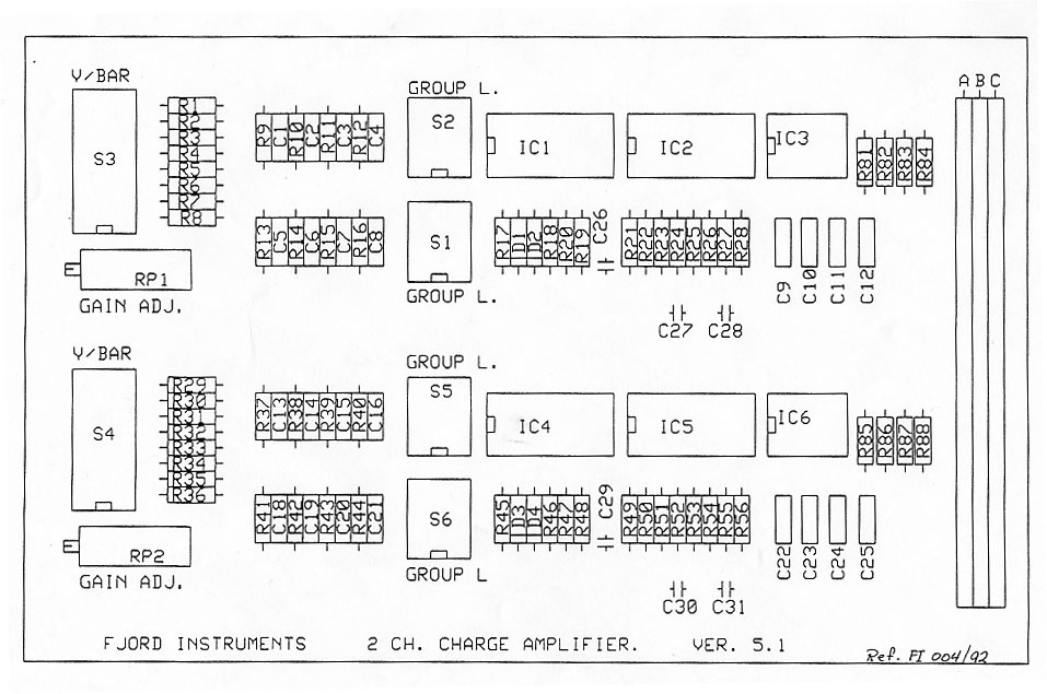
Fig. 5. Charge Amplifier PCB layout diagram. Click to enlarge.
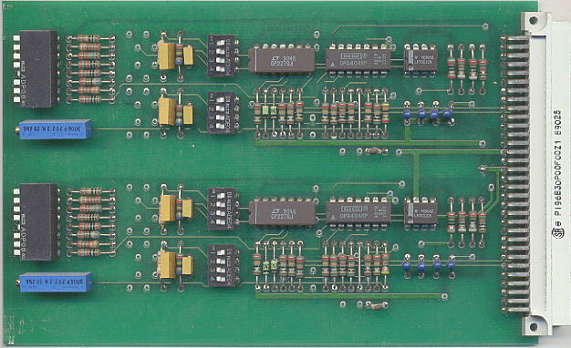
Fig. 6. Charge Amplifier Printed Circuit Board (PCB)
3.5: 12.5 m GL vs. 25 m GL
The Charge Amp cards in the rack now have the following configuration. It's unmodified since last time this system was used, during ODEN's 1996 Arctic Expedition, with a 3 * 100 m HSSG, 12.5 m GL configuration.
Cards 1 to 14 (2 spares) - counted from left in the section below the equalizer cards - have resistors and capacitors mounted in component position (ref. fig. 5) C2, C6, C14, C19 and R10, R14, R38, R42 so that setting switch 3 on Group Length DIL switches S1, S2, S5 selects 12.5 m Group Length on an HSSG streamer section with SG = 68 V/Bar and CG = 45 nF.
|
The streamer is now set to 25 m GL by changing program module plugs in the middle of each streamer section. Assuming switch 3 on Group Length DIL switches S1, S2, S5, S6 is set ON the gain is then doubled (check the gain equation - CG is increased from 45 nF to 90 nF). We then have a conversion table:
| Gain select DIL
Switch S3, S4 [Position] |
Gain (Sensitivity) NORMAL: 12.5 m GL, HSSH [V/Bar] |
Gain (sensitivity) 25 m GL, HSSG [V/Bar] |
|---|---|---|
| 2 | 10 | 20 |
| 3 | 15 | 30 |
| 4 | 20 | 40 |
| 5 | 25 | 50 |
| 6 | 50 | 100 |
| 7 | 75 | 150 |
| 8 | 100 | 200 |
4. Power supply tips & tricks
The power supply consists of two Schroff power units with the following specs:
- Model PSG-218
- Part no. 11005-155
- Dual power O/P V1 and V2
- V1, V2: 18 VDC, max. 1.2 A
Each power unit supply one "shelf" of the rack where the charge amp cards are placed (the equalizer cards are passive). Having only 24 channel recording all 12 involved charge amp cards (remember, 2 channels per card) are all placed on the same shelf. If there is a failure in the supply that feeds these cards just rewire the cables in the power supply subrack. It's easy to disconnect the wires from the power supply units. Note that you cannot simply move the cards to the shelf with the still working supply voltages - what about the channels that's coming from the equalizer?
5. How do I test it?
In the field these items should be available:
- A signal generator, signal range must at least cover 10-150 Hz, 0.1 - 1 VP-P
- Instruments depending on test method:
- An oscilloscope: Tek THS-710 with floating input channels (important!!)
- Multimeter with relative dB ac-voltage measurement capability.
- A single-ended-to-differential converter, output via capacitors so that it mimics a hydrophone group. Unit used here acts as a voltage source with capacitive output impedance, C = 110 nF
- Power supply, dual, adjustable.
- Probes etc.
|
Circuit schematics for the single-to-differential converter is shown below. U1A is a unity gain inverting amplifier. U1B is identical but for the offset and gain adjustment pot.meters. Using component values from C1-C4, it acts as a voltage source with a capacitive output impedance of 100 nF. A unity gain buffer stage was later added (not shown) and the output impedance altered to 110 nF.
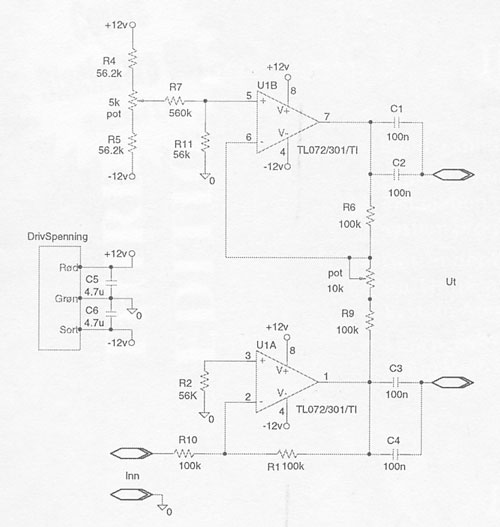
Fig. 7. Single ended to differential converter (modified, see text).
Set signal generator to 40 Hz sinusoid, 100 mVP-P (meaning peak-to-peak) amplitude, or ± 50 mV. Route signal generator output to single-to-differential converter input (note: this raises signal amplitude by 2). Take output from this unit to selected channel pins on Charge Amp system input connector, see pin-out diagram below. Output from charge amp to scope channel 2 (must be floating with respect to channel 1 and ground). Set gain switch on card front to 100 V/Bar. Group Length DIL switches must be set to position 3 (HSSG, 12.5 m GL). Now, what signal amplitude to expect?
First calculate modified S01 due to altered CG = 110 nF, using the equation in section 3.2. From earlier we have CF = 63 nF and SG = 68 V/Bar.
S01 = (2*110 nF*68 V/Bar)/63 nF = 237.5 V/Bar
yielding gain factor A:
A = (237.5 V/Bar) / (68 V/Bar) = 3.49
This gain factor must be multiplied by two due to the single-to-differential converter, thus we have a total gain factor of:
3.49 * 2 = 7.0
So, to answer the question, a 40 Hz sinusoid, 100 mVP-P from the signal generator should yield a 700 mVP-P output signal.
The trimpot. on the front can be used to perform gain adjustments.
Actually, the circuit diagram of the charge amplifier is a bit more complicated, but our conclusion should still be valid. We haven't looked into the gain stage associated with the tapped resistor ladder (R1-R8 on ch. 1) and the unity gain (R25 is a strap!) single-to-differential stage that follows. And measuring the cutoff filter effect was not mentioned. Please refer to the manual - the part list is needed if one seeks a thorough understanding of the Charge Amp's inner workings ...
An alternative approach is to use a Multimeter with a relative voltage gain measurement capability. First make the input signal a 0 dB reference by pushing the REL button. Then measure the output signal. A gain of 7 is equal to 20*log(7) dB = 16.9 dB.
A proper lab. test could be performed with a signal analyzer, e.g. an HP-3562A Dynamic Signal Analyzer, producing plots of amplitude- and phase response as a function of frequency.
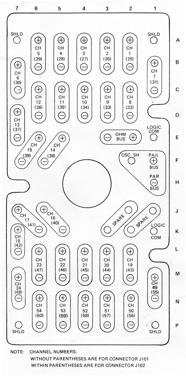
Fig. 8. Pin-out signal input/output connector. Click to enlarge.
6. Manual
56 channel Equalizer and Charge Amp. system manual (pdf, 652 kB).
University of Bergen
Institute
of Solid Earth Physics
Allé gt. 41, N-5007 Bergen, NORWAY
Tel: (+47) 5558 3420 Fax: (+47) 5558 9669
Email: Yngve.Kristoffersen@ifjf.uib.no